
Overview
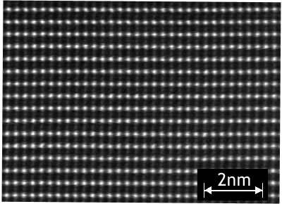
KTN crystal is an oxide crystal composed of potassium (K), tantalum (Ta), and niobium (Nb), and has the greatest EO (Electro-optic) effect among existing materials.
Using this large EO effect (Kerr effect), it is possible to create compact optical scanners (optical deflectors) with no moving parts, varifocal lenses, and efficient phase modulators.
We sell optical devices using KTN crystals such as optical scanners and varifocal lenses, OCT light sources for optical scanner application products, and KTN crystal chips for research and new device applications.
Niobium-free oxide lens material KT (KTaO 3) for crystals here please look at.
feature
>> Large EO effect (s11~=3.0×10⁻¹⁵ m 2 /V 2, ex: δn~0.003 *Conditions below)
*ε r = 17500, 400 V/mm, wavelength 633 nm according to our research
>>Wide usage wavelength range
(The wavelength range in which the EO effect can be used is 488 nm to 3500 nm, and it is a transparent single crystal with an internal transmittance of almost 100%.)
application
- Optical deflector
- Variable focus lens(jump to our English site)
a) Klaus C. Gwosch, Jasmin K. Pape, Francisco Balzarotti, Philipp Hoess, Jan Ellenberg, Jonas Ries and Stefan W. Hell
“MINFLUX nanoscopy delivers 3D multicolor nanometer resolution in cells”,
Nature Methods, volume 17, 217–224, 2020.
b) Jasmin K. Pape, Till Stephan, Francisco Balzarotti, Rebecca Büchner, Felix Lange, Dietmar Riedel, Stefan Jakobs and Stefan W. Hell,
“Multicolor 3D MINFLUX nanoscopy of mitochondrial MICOS proteins”,
Proc. Natl. Acad. Sci. USA, published August 11, 2020.
- optical modulator
- For various research (chips, devices)
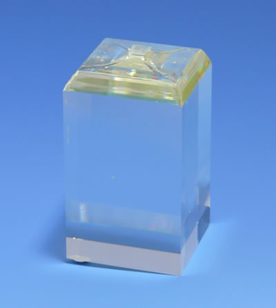
KTN crystal chip
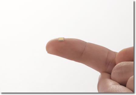
KTN crystal chips can also be processed in terms of size and shape based on the customer's device design. Also, please feel free to contact us regarding T C (phase transition temperature), electrodes, anti-reflection coatings, etc.
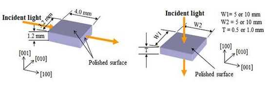
The following sizes are in stock, so we can offer them at an affordable price.
| Size (unit: mm) | polished surface |
|---|---|
| 4.0×3.2×1.2 | 4 side mirror polishing |
| 5.0×5.0×1.0 | 2 side mirror polishing |
| 10×10×0.5 | 2 side mirror polishing |
 close up