
What is a nitride semiconductor epitaxial wafer?
Power devices using nitride semiconductors are expected to be green devices that support the future low-carbon society.
NTT-AT contributes to the early realization of energy conservation with its nitride semiconductor epitaxial wafer manufacturing technology.
Do you have any of these issues in the development of power devices?
- I want to try various types of substrates that have not decided which type of substrate to use.
- We would like to secure a future mass production system while doing trial production with a small amount of various products.
- Of course, a large diameter size is also required.
Nitride semiconductor epitaxial wafers from NTT-AT
- We have the technology to grow crystals on silicon (Si), sapphire (Al2O3), silicon carbide (SiC), and gallium nitride (GaN) substrates, and can handle all substrates used for nitride systems. Development studies using multiple substrate types can be carried out in parallel. We do not waste your valuable time.
- We accept orders from small-scale prototypes to mass production.
- It is also compatible with large-diameter 8-inch silicon substrates. In addition, device fabrication and material analysis are also possible through collaboration with our related departments.
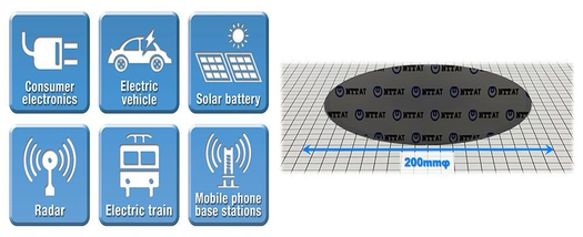
Application example
- USB small quick charger
- LED street light
- Power devices for mobile base stations
- Automotive power device
- Power devices for home appliances
- Environmentally resistant device
HEMT structure for Power application (on 6 inch Si)
There are products available for immediate delivery. Please contact us.
Click the desired Part Number to display the inquiry form.
Sorry to trouble you, but please write [Part Number] and [Quantity] in the request column.
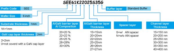
| Part number | GaN cap | AlGaN barrier | AlN | Channel | |
|---|---|---|---|---|---|
| Content | Thickness | Spacer | |||
| SEE61K22227S20G | 2nm | 0.22 | 27nm | 1nm | 200 nm |
| SEE61K22227S30G | 2nm | 0.22 | 27nm | 1nm | 300nm |
| SEE61K22515S30G | 2nm | 0.25 | 15nm | 1nm | 300nm |
| SEE61K22520S30G | 2nm | 0.25 | 20 nm | 1nm | 300nm |
| SEE61K22525S30G | 2nm | 0.25 | 25nm | 1nm | 300nm |
| SEE61K23020S30G | 2nm | 0.30 | 20 nm | 1nm | 300nm |
| SEE61K21745N30G | 2nm | 0.17 | 45nm | - | 300nm |
| SEE61K22520N30G | 2nm | 0.25 | 20 nm | - | 300nm |
| SEE61K22520N35G | 2nm | 0.25 | 20 nm | - | 350 nm |
| SEE61K22520N40G | 2nm | 0.25 | 20 nm | - | 400nm |
| SEE61K22526N15G | 2nm | 0.25 | 26nm | - | 150nm |
| SEE61K22526N20G | 2nm | 0.25 | 26nm | - | 200 nm |
| SEE61K22526N35G | 2nm | 0.25 | 26nm | - | 350 nm |
| SEE61K22527N35G | 2nm | 0.25 | 27nm | - | 350 nm |
| SEE61K23020N30G | 2nm | 0.30 | 20 nm | - | 300nm |
| SEE61K02822S30G | - | 0.28 | 22nm | 1nm | 300nm |
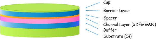
| cap layer | |
|---|---|
| Materials | GaN |
| Thickness | 2 (nm) or no cap |
| Barrier | |
| Materials | AlGaN |
| Al content | 20~30 (%) |
| Thickness | 15~27 (nm) |
| Channel | |
| Materials | GaN |
| Thickness | 150~400 (nm) |
| Buffer | |
| Doping | C-doping |
| Thickness | ~3900 (nm) |
| Substrate | |
| Silicon | 1mm thickness |
| Features | |
| Sheet resistance: 350~400 ohm/sq. (w/ AlN spacer), 450~500 ohm/sq. (w/o AlN spacer) Electron Mobility: ~1700 to 1900 cm2 /Vs FWHM (002): <800 arcsec FWHM (102): <1400 arcsec Breakdown voltage: 800V – 1000V (depending on the device structure) Bowing value: < 50um |
|
AlGaN/GaN HEMT structure epitaxial product (example)
| cap layer | Material: GaN | |||
|---|---|---|---|---|
| doped or undoped | ||||
| Thickness: 0-5nm | ||||
| Barrier layer | Material: AlGaN with or without AlN spacer | |||
| doped or undoped | ||||
| Al-content: 10-50% | ||||
| Thickness: <~50nm | ||||
| Buffer layer | Material: (Al)GaN | |||
| Thickness: 1-3 μm | ||||
| Substrate | Si | Sapphire | SiC | GaN |
| 2 to 8 inches | 2 to 3 inches | 2~6 inch | 2 to 4 inches | |
Lineup available ( 6 inch & 8 inch )
| on Si substrate | AlGaN/GaN HEMT structure | |
|---|---|---|
| 6 inch | 8 inch | |
| GaN cap | ✔ | ✔ |
| in-situ SiN (~5nm) | ✔ | ✔ |
| in-situ SiN (~40nm) | ✔ | ✔ |
|
p-GaN (~80nm)
(Mg: 2x1019 cm-3) |
✔ | ✔ |
catalog download
| "InAlN/GaN HEMT Epi Wafer" Catalog | 824KB | PDF download |
|---|---|---|
| "GaN EPITAXIAL WAFERS" catalog (English) | 3.8MB | PDF download |
Data material "Expected to improve device manufacturing yield - 8-inch AlGaN/GaN epitaxial wafer with excellent uniformity"
If you are interested, please use the inquiry form.
Request for data materialsIf you are interested, please use the inquiry form.
For other information requests and inquiries, please use the inquiry form.
Request for materials / inquiriesRelated services
For customers who want to perform structural analysis or component analysis on this product or prototype device
- Morphological observation for device and material morphology, structure, and crystal structure analysis
- Chemical analysis from trace analysis of inorganic and organic fields to principal component analysis
For customers who want to outsource the device prototyping process
*This product has been classified under Item 7(18) in the Export Control Order Attachment List 1 by Japan's Ministry of Economy,
Trade and Industry (METI), and a license from METI is required for its export.
*The contents of this website are subject to change without notice due to product improvements.
 close up