
Promote your research and development and realize your ideas! !
Features of our silicon waveguide fabrication service
Fabrication of silicon waveguides based on customer designs
高度加工技術に支えられたSi細線導波路ベースのプラットフォーム上にお客様の設計に基づいた極微細光回路を実現します。
※ 設計図( GDSⅡ形式 もしくは dxf 形式)をご用意ください。
Achieves low-loss connections between silicon waveguides and optical fiber arrays
spot size converter, it enables low-loss connection with an optical fiber, etc., enabling customers to perform high-precision evaluations.Equipped with a
Capable of meeting various design needs
We offer options to meet the diverse needs of our customers, such as precise control of optical properties and composites with different types of materials such as polymers.
Seamless support from silicon waveguide fabrication → characteristic evaluation → optical fiber mounting
In addition to fabricating silicon waveguides, we can seamlessly respond to requests from customers, from evaluating optical characteristics to attaching optical fibers to chips.
- Basic prototype chip example
- spot size converter
- Option processing example
- Mounting with optical fiber
- Document Download / Inquiry
1. Si wire waveguide - example of basic prototype chip production -
We realize ultrafine optical circuits based on customer designs on Si wire waveguide-based platforms.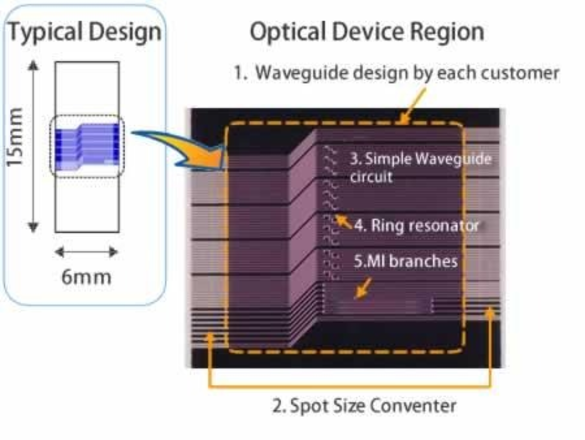
| Waveguide core diameter | 400-500nm width x 220nm thickness |
|---|---|
| ring resonator gap | 150 nm or more |
| waveguide region | 5mm x 5mm |
| SS conversion core diameter | 3μm×3μm |
| SS converter waveguide spacing | 50 μm or more |
| Chip cutting size | 15mm x 5.6mm |
2. Low loss connection: spot size converter
By adding spot size conversion to the end of the waveguide, it can be connected to an optical fiber or laser with low loss. (1.5[dB/connection])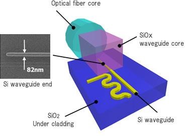
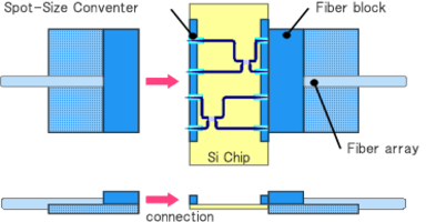
Example of connecting an optical fiber array to a Si chip
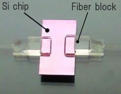
Fiber array connection structure
3. Example of optional processing
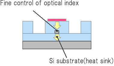
- Heater for temperature control and additional wiring
- Controls the transmission wavelength by controlling the refractive index with high precision.
- Introduction of functional materials
- Introduction of functional materials such as polarized materials.
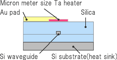
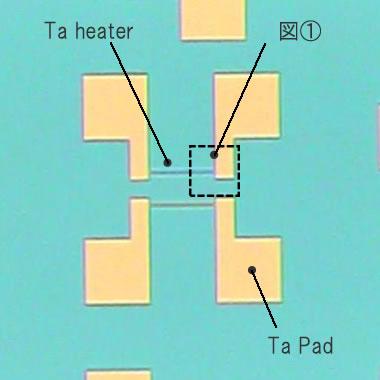
Minimal Ta heater for temperature control
| Application example |
|
○ Optical switch, precision wavelength filter |
| Customer request |
|
○ Precise control of optical properties by local heating |
| solution |
|
a high-melting-point metal Ta thin film.1Achieves a heater that is hard to break by using 2 Ultra-fine heater realized by high-precision shape processing 3 Heating only specific parts is realized by routing with low resistance Au wiring |
Example of Ta heater pattern processing on quartz (over clad)
Application example
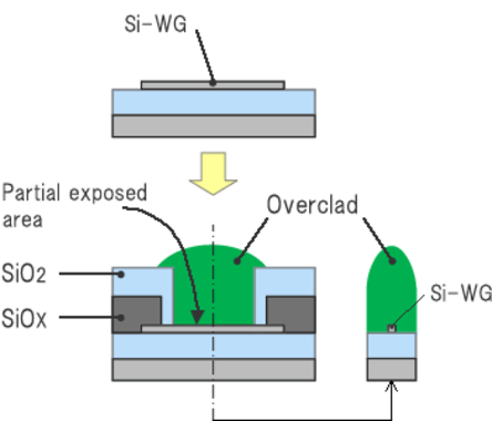
Introduction of functional materials
Overcladding can be formed using various functional materials.| Application example |
|
○ Sensors, modulators |
| Customer request |
|
○ Hybridization of Si waveguides and functional materials |
| solution |
|
1 Realization of partially exposed structure of Si waveguide 2 Applying processing that does not damage the Si waveguide by combining dry etching and wet etching 3 Realization of a process that does not partially form overcladding |
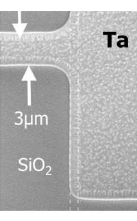
 close up