Transmission Electron Microscopy (TEM)
[Gallery]
Examples of advanced TEM observations are shown. We also support TEM related simulations, which make possible better understanding of microscopic nature of various materials.
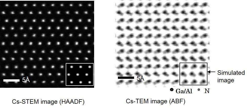
Gallium Nitride (GaN)
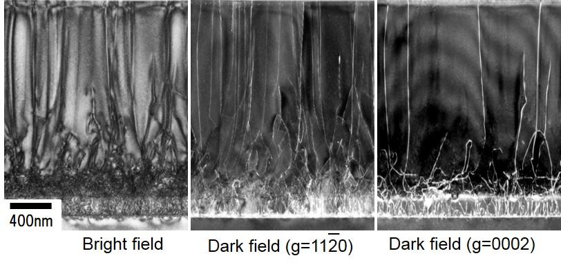
Dislocations
Type of dislocations (edge, screw, or/and mixed) is identified by comparison of dark-field and bright-field TEM images.
Polarity
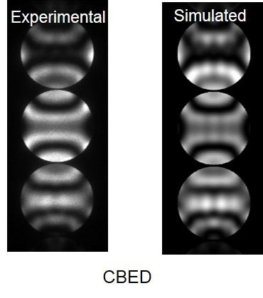
Local polarity (direction of crystal growth) of AlGaN is determined from CBED patterns and STEM images, where simulations are emplyoyed, and thus simulated images are superimposed on the experimental images in order to derive the polarity.
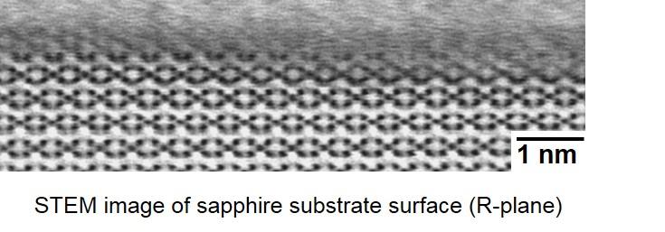
Substrate (Sapphire)
TEM/STEM images show atomic/molecular level states of substrate surfaces/interfaces.
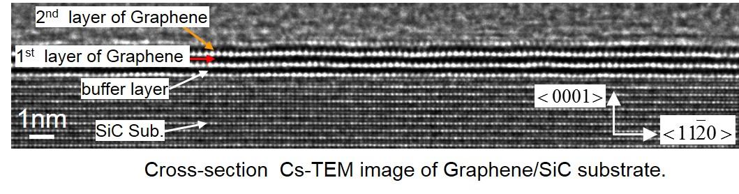
Graphene
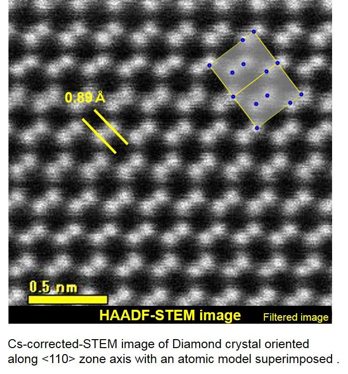
Diamond Crystal
A point resolution of 86 pm in the real image, not Fourier transformed image is attained.