
May 16, 2017
Development of a highly stable wavelength tunable light source for thickness measurement using a KTN crystal
HPK, NTT-AT and NTT have developed a wavelength tunable light source suitable for measuring the thickness of silicon wafers used in power devices. The light source can sweep the wavelength by changing the incident angle of the light to an optical grating in a laser cavity by using a KTN laser beam deflector.
In a joint partnership, we have been developing and selling a wavelength tunable light source using the KTN deflector developed by NTT for use in optical coherence tomography (OCT). We have now developed a light source for thickness measurement systems used in factories that produce silicon wafers for power devices.
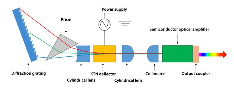
Configuration of KTN-based wavelength swept light source.
Since current wavelength tunable light sources used in OCT employ mechanical moving mirrors for wavelength tuning, they are susceptible to vibrations of the system. The newly developed product has eliminated mechanically moving parts by using a KTN deflector. Consequently, it is less susceptible to vibrations and can continue to operate stably over a long period. By improving the material and temperature control, we have reduced the influence of the ambient temperature on measurements and achieved high reproducibility. In addition, a blue LED light makes KTN operation stable within a short time. Using this property, we have reduced the starting time. Moreover, by setting the central wavelength of the light source at 1.3 μm with relatively low dopant absorption, the thickness of highly doped silicon wafer can be measured with a high degree of accuracy. The semiconductor optical amplifier used in this product has been developed by NTT Electronics Corporation, an NTT Group company. It operates at a central wavelength of 1.3 μm and is made highly reliable by improving the hermetic seal.
We will apply the product to medical and industrial fields by further improvements of its performance such as operation speed and wavelength tuning range.

